| |
|
|
|
|
|
|
|
|
|
|
|
|
|
|
 |
|
 |
 |
|
||||||||||
|
|
|
|
|
|
|
|
|
|
|
|
||||
|
|
|
|
|
|
|
|
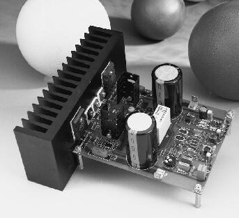
IGBT audio amplifier |
T. Giesberts
|
| This is a first class amplifier that provides
excellent music reproduction, which is evidenced not so much by measurement
as by audition. To some listeners, it has a quality not unlike that of
a valve amplifier. The power output of this IGBT amp is 90 W into 8 Ohm
(about 160 W into 4 Ohm).
IGBT amplifier brief technical data: Fig. 1. Circuit diagram of the IGBT amplifier. Circuit description: The circuit diagram of the IGBT amplifier is given in Fig. 1. To improve performance at high frequencies, a damping resistor is added in inductor L1. A symmetrical design has the advantage that it minimizes problems with distortion, particularly that associated with even harmonics. Therefore, the input stages consist of two differential amplifiers, T1-T2 and T3-T4. These use discrete transistors, not expensive dual devices, to keep the cost down. Performance is excellent, particularly if the transistors are matched. A differential amplifier is one of the best means of combining two electrical signals: here, the input signal and the feedback signal. The amplification of the stage is determined mainly by the ratio of the collector and emitter resistances (in the case of T1-T2 these are R9, R10, R11 and R12). These provide a form of local feedback: limiting the amplification reduces the distortion.
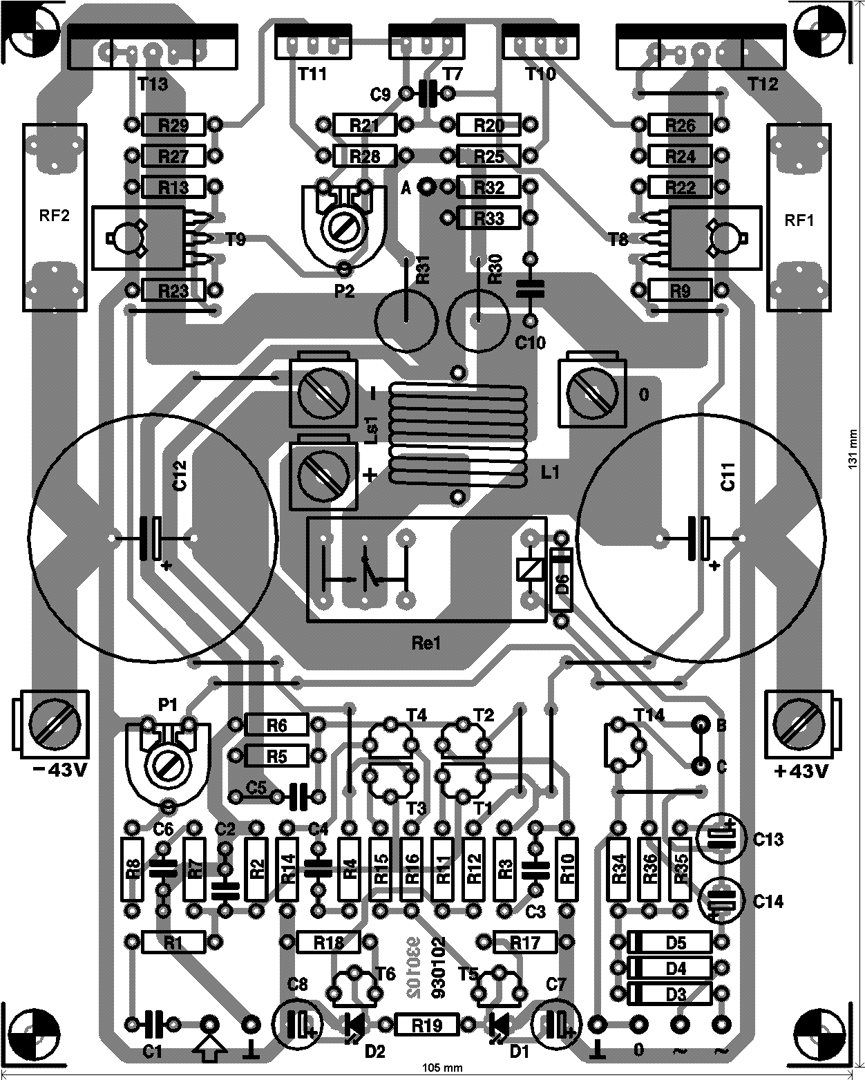
Two RC networks (R3-C3 and R4-C4) limit the bandwidth of the differential amplifiers and these determine, to a degree, the open-loop bandwidth of the entire amplifier. The d.c. operating point of the differential amplifiers is provided by two current sources. Transistor T6, in conjunction with R18 and D2, provides a constant current of about 2 mA for T1-T2. Transistor T5, with R17 and D1, provides a similar current for T3-T4. The combination of a transistor and an led creates a current source that is largely independent of temperature, since the temperature coefficients of the led and the transistor are virtually the same. It is, however, necessary that these two components are thermally coupled (or nearly so) and they are, therefore, located side by side on the printed-circuit board. In the input stage, C1 is followed by a low-pass section, R1-C2, which limits the bandwidth of the input to a value that the amplifier can handle. Resistor R2 is the base resistor of T1 and T3. So far, this is all pretty normal. Network P1-R7-R8 is somewhat out of the ordinary, however. It forms an offset control to adjust the direct voltage at the output of the amplifier to zero. Such a control is normally found after the input stage. The advantage of putting it before that stage is that the inputs of the differential amplifiers are exactly at earth potential, which means that the noise contribution of their base resistors is negligible. The signals at the collectors of T1 and T3 are fed to pre-drivers T8 and T9. Between these transistors is a 'variable zener' formed by T7 which, in conjunction with P2, serves to set the quiescent current of the output transistors. The output of the pre-drivers is applied to T10 and T11, which drive IGBTs T12 and T13. This power section has local feedback (R30-R31). The design of T10,T13 is a kind of compound output stage, since the collector of the power transistors is connected to the output terminal. The voltage amplification is limited to x3 by the local feedback resistors (R30-R31). Here again, this feedback serves to reduce the distortion. The overall feedback of the amplifier is provided by R5-R-C5. Electrolytic capacitors C11 and C12 (10,000 µF each and part of the power supply) are located close to the IGBTs, so that the heavy currents have only a short path to follow. At the output is a Boucherot network, R32-R33-C10, that ensures an adequate load on the amplifier at high frequencies, since the impedance of the loudspeaker, because of its inductive character, is fairly high at high frequencies. Inductor L1 limits any current peaks that may arise with capacitive loads. The signal is finally applied to the loudspeaker, LS1, via relay contact Re1. The relay is not energized for a few seconds after the power is switched on to obviate any plops from the loudspeaker. Such plops are caused by brief variations in the direct supply voltage arising in the short period that the amplifier needs to reach its correct operating level. Fig. 2. Circuit diagram of the power supply for one mono IGBT amplifier. The supply voltage for the relay is derived directly from the mains transformer via D3 and D4. This has the advantage that the relay is deactuated, by virtue of the low value of C13, immediately the supply voltage fails. The delay in energizing the relay is provided by T14 in conjunction with R36 and C14. It takes a few seconds before the potential across C14 has risen to a value at which T14 switches on. This darlington transistor requires a base voltage of not less than 1.2 V before it can conduct. The power supply (see Fig. 2) is traditional, apart from the resistors, R5-R8, in the power lines. These limit, to some degree, the very large peak charging currents drawn by electrolytic capacitors C11 and C12. Moreover, together with these capacitors, they form a filter that prevents most spurious voltages from reaching the amplifier. Measurements on the prototype showed that this was particularly evident at frequencies below 500 Hz. Fig. 3a. Printed-circuit board for the IGBT amplifier. Fig. 3b. Partlist IGBT amplifier. Fig. 3c.Track layout for the IGBT amplifier. (131x105 mm) Here you find how to make your own PCB's (Printed circuit boards): How to make printed circuit boards (PCBs) Fig. 4. Good thermal coupling between the transistors and the heat sink ensures a long life of the devices. (Click on the link for details of the thermal coupling)
Construction: The design of the printed-circuit board for the amplifier (Fig. 3) takes good account of the large currents that flow in the amplifier. This has given rise to a couple of tracks being paralleled instead of combined, so that the effect of currents in the power section on the input stages is minimal. Populating the board is straightforward. Although not strictly necessary, it is advisable to match the transistors used in the differential amplifiers. This may be done conveniently on an hfe tester by measuring the amplification at a collector current of about 1 mA. If such a tester is not available, use a base resistor that results in a collector current of about 1 mA measured with a multimeter. With the same resistor, test a number of other transistors and note the collector currents. Take care: The hfe of the transistors is temperature dependant. When you touch the transistors with your fingers the temperature of the transistor rises and the hfe changes. To match the transistors accurately the same temperature must be maintained. Mount the selected pairs on the board and pack them closely together with a 5 mm wide copper ring (made from a piece of 12 mm copper water pipe). Inductor L1 consists of six turns, inner diameter 16 mm (5/8 in), of insulated copper wire 1.5 mm (1/16 in) thick. Mount RL1 inside the coil. The large transistors are located on one side of the board, so that they can be fixed directly to the heat sink. They must be insulated from the heat sink with the aid of ceramic washers. Connections from the power supply and to the loudspeaker are by means of terminal blocks that can be screwed on to the board. Fig. 5. Wiring of the IGBT amplifier. Mount the two amplifier boards, mains transformers and electrolytic capacitors in a suitable enclosure. The wiring diagram for one channel is given in Fig. 5. It is advisable to measure the supply voltages before they are applied to the amplifiers. Also, turn P2 to maximum (wiper towards R33) before connecting the power supply to the amplifiers. Set input presets P1 to the centre of their travel. A few seconds after the supply has been switched on, the relay should come on. Connect a multimeter (1 V direct voltage range) and adjust P1 until the meter reads zero (both channels!). Switch the supply off again and connect a multimeter (100 mV d.c. range) across RF1 or RF2. Switch on the supply and adjust P2 for a meter reading of about 10 mV: this corresponds to a quiescent current of 100 mA through T12 and T13. After about half an hour, the current will have stabilized at about 200 mA (meter reading of about 20 mV). Readjust P2 slightly if required. Note that owing to the positive temperature coefficient of IGBTs, the quiescent current does not increase but drop with rising dissipation. Finally, recheck the direct voltages at the outputs of the amplifiers and, if necessary, readjust P1 slightly.The loudspeakers must be 4-ohm or 8-ohm types, whose impedance must not drop below 3 Ohm. It is not permissible to connect two 4-ohm units in parallel to the amplifier, because that would give problems when large drive signals are applied to the IGBTs. Fig. 6. Mains switch-on delay. The circuitry of the 'black box' (in dashed lines) in Fig. 2 is shown above. It may be asked what the function of it is, since there is already a power-on delay in the amplifier itself. That delay serves to obviate plops and clicks caused by switching; it connects the loudspeakers to the amplifier only after this has had a short period of 'settling down'. The mains switch-on delay is intended to switch on the mains gradually with heavy loads, so that the fuses do not blow. In the circuit, a number of power resistors, R3,R6, are connected in series with the mains supply lines to limit the current at switch-on to 5 A. When the mains is switched on with S1, only relay Re1 is energized in the first instance, so that the current must flow through the power resistors. When after a few seconds capacitors C4 and C5 have been charged, relay Re2 is also energized, whereupon the power resistors are short-circuited by the relay contacts. These few seconds allow the buffer capacitors in the power supply to be charged at a reasonable rate, so that high currents are prevented. The relay coils are connected in series and are energized directly by the mains via bridge rectifier B1, impedances ZC1 and ZC2, and R1. The value of C1 and C2 depends on the current required by the relay coils and the level of the mains voltage. The specified 24V Siemens V23056-A0105-A101 relays are rated at 30 mA. C1,C2 should have a rating of 630 Vdc / 250 Vac for 110V / 60 Hz : C1=820 nF, C2=330 nF for 220V / 50 Hz : C1=330 nF, C2=220 nF for 230-240V / 50 Hz : C1=470 nF C2=omitted Fig. 6a. Printed-circuit board for Mains switch-on delay. Fig. 6b. Track layout for Mains switch-on delay. (75x136 mm) |
|


|
|